Download Images Library Photos and Pictures. Physical Design Flow V: Physical Verification – VLSI Pro PDF) Antenna avoidance in layer assignment PDF) Factor analysis of plasma-induced damage in bulk FinFET technology Special Cells used in VLSI Physical Design

. Antenna Effect Prevention Techniques in VLSI Design - YouTube Physical Design Flow V: Physical Verification – VLSI Pro Antenna Effect in 16nm Technology Node

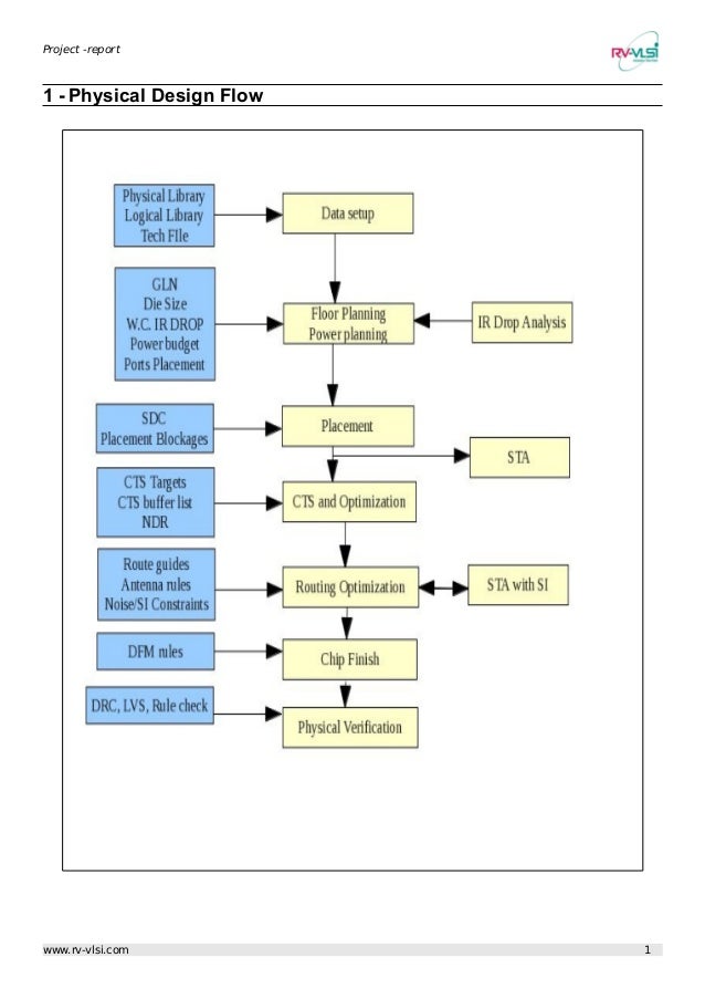
Routing optimization and Chip Finishing - Physical design, STA & Synthesis, DFT, Automation & Flow Dev, Verification services. Turnkey Projects

Antenna effect in VLSI Fabrication | Plasma Induced Gate Oxide Damage | Plasma Etching - YouTube
 ⨘ } VLSI } 8 } Antenna Effects } - YouTube
 Team VLSI: Antenna Prevention Techniques in VLSI Design
 Antenna violations resolved using new method - EDN
 Before metal 2 is constructed, the charging on the wire segment (C, D)... | Download Scientific Diagram
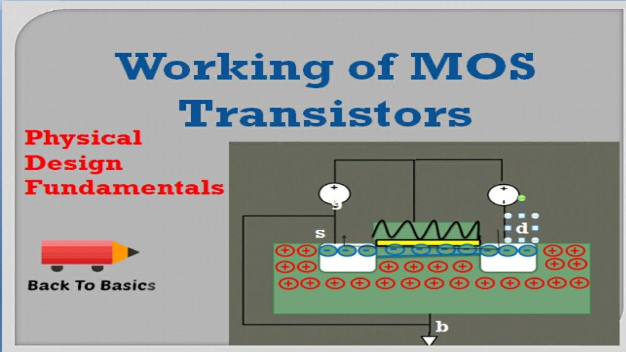 Antenna Effects | Physical Verification | Back To Basics - YouTube
 VLSI Backend Design: Antenna Effect

 Detection of an antenna effect in VLSI designs | Semantic Scholar
 Antenna effect: Do the design rules really protect us? | EE Times
 Team VLSI: Antenna Prevention Techniques in VLSI Design

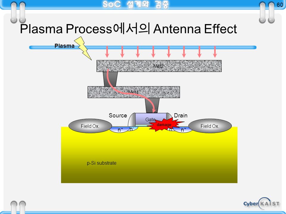 경종민 1 VDSM and Full-Custom Layout Design Issues(2) - ppt download
 Vlsi
Vlsi

 Process Antenna Rule – sarvangsanghavi
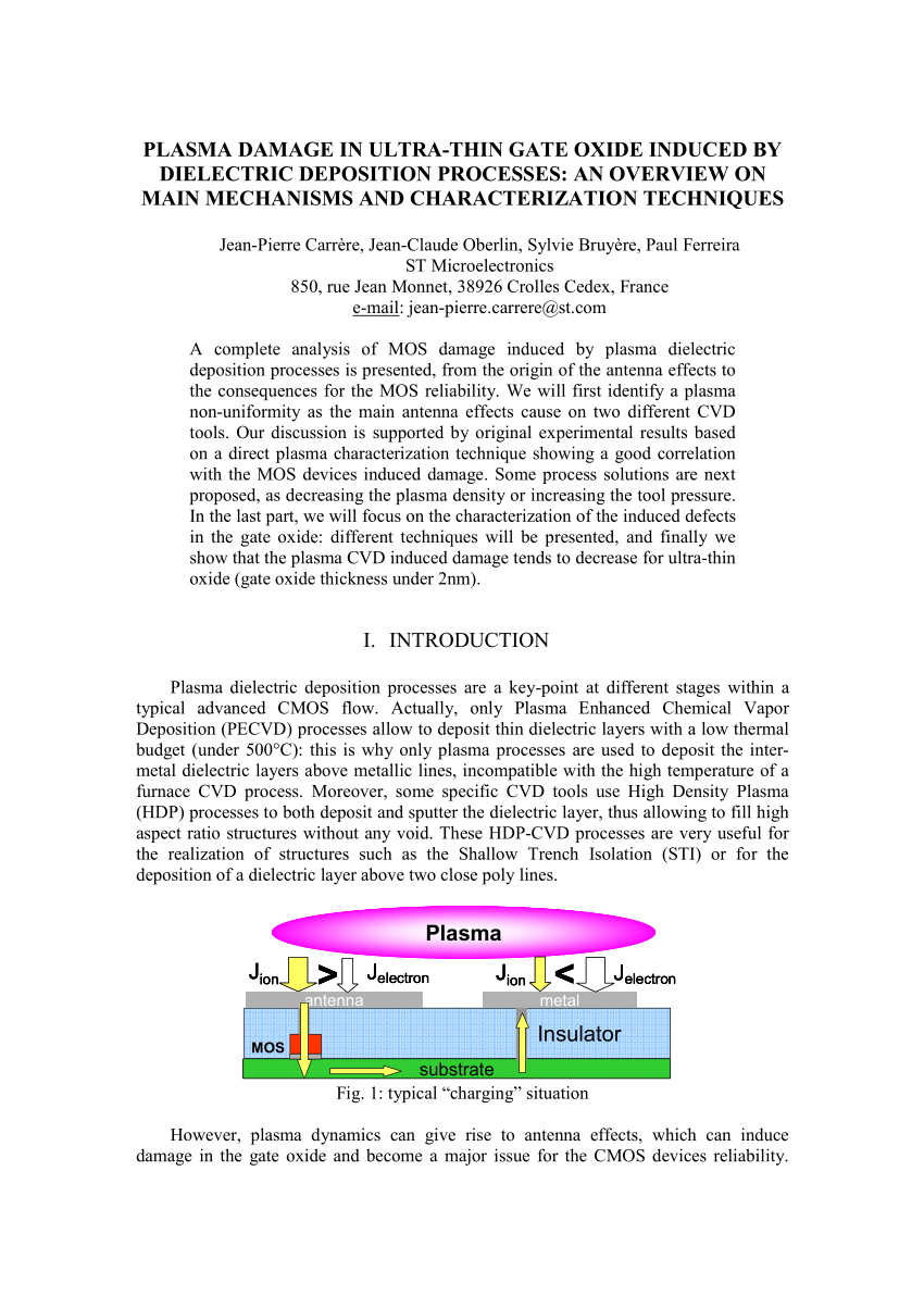 PDF) Plasma Damage in Ultra-Thin Gate Oxide Induced by Dielectric Deposition Processes: An Overview on Main Mechanisms and Characterization Techniques
Antenna Effects | Physical Verification | Back To Basics - YouTube
 PDF) Antenna avoidance in layer assignment
 Antenna Effect Prevention Techniques in VLSI Design - YouTube
 Mitigating antenna effect in IC design(2)
 Antenna Effect Prevention Techniques in VLSI Design - YouTube

 Antenna Effects | Physical Verification | Back To Basics - YouTube
 Antenna Effects | Physical Verification | Back To Basics - YouTube

 Design rule checking - Wikipedia
 pramod
Comments
Post a Comment